
UniRank Places BGSBU at third place In Jammu and Kashmir

- Sep 12, 2021 |
- BGSBU
UniRank in its latest ranking placed Baba Ghulam Shah Badshah University Rajouri...
Read More →The Department offers PCB fabrication facility to various Engineering Graduates at various stages of Major Projects (Phase 1 and 2) established in 2012-13. In addition to that fabrication facility is utilised in Printed Circuit Board laboratory as a part of Electronics and Communication Engineering curriculum. The facility of PCB fabrication is also extended for other branches like ERE and CSE/ITE whosoever intend to design PCB at College level. A state of art instruments facility includes;
1. PCB prototype machine is available at the fabrication facility of Electronics and Communication Engineering department. EP2006 series PCB Prototype Machine will make the most simple, quick precise way to make own PCB prototype with an input of Gerber file, PCB can be made within minutes to hours. The main features of PCB prototype machine are;
a) High accuracy and easy operation.
b) Automatic tool Length Detect Function.
c) Surface detect and real time working depth compensation function.
d) Working depth setup by software control.
e) Motorized Z – axis with software control drill speed.
2. Licenced TINA software is available at the fabrication facility so that its outlay of PCB can be simulated for final fabrication.
3. The equipment for manual PCB development process available at facility includes;
a). The PCB artwork film maker is used as a contact printer for creating design films from the PCB Layout.
b). The artwork table for manually designing the films and for correcting or changing the existing films.
c). The shearing machine for cutting the PCB according to film size.
d). The photoresist dip coating machine for coating photoresist on the PCB Laminate.
e). UV exposure machine used for exposing photoresist coating, the PCB and films.
f). After exposing the Development tank for removing unused photoresist.
g). The dye tank for highlighting the design of PCB.
h). The etching machine for removing unused copper from the PCB.
i). The drilling machine for making the holes in the PCB.
j). The PCB design kit including tapes, stencils and other accessories used for designing the PCB.
UniRank in its latest ranking placed Baba Ghulam Shah Badshah University Rajouri...
Read More →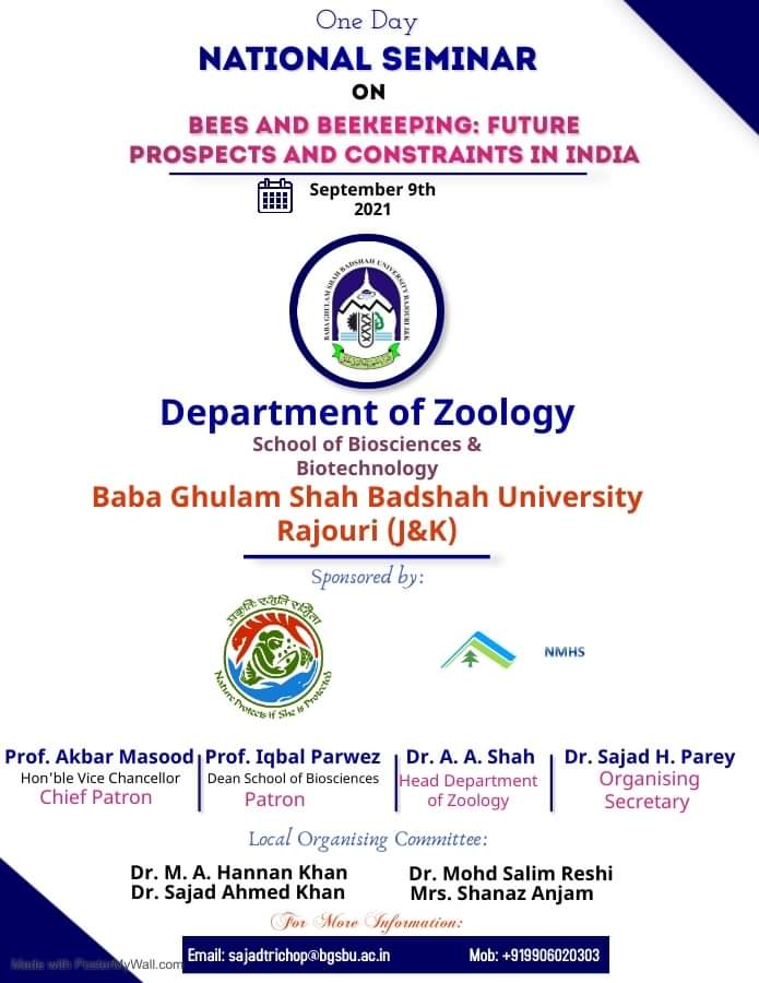
BGSBU organises National Seminar on Beekeeping
Read More →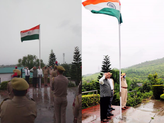
BGSBU celebrates 75th Independence Day
Read More →